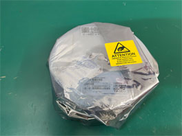

Step1: Product

Image shown is a representation only


| Attribute | Value |
|---|---|
| Tab | Tab |
| PPAP | No |
| SVHC | Yes |
| EU RoHS | Compliant with Exemption |
| Category | Power MOSFET |
| Mounting | Through Hole |
| ECCN (US) | EAR99 |
| Pin Count | 3 |
| Automotive | No |
| PCB changed | 3 |
| Availability | In Stock |
| Channel Mode | Enhancement |
| Channel Type | N |
| Configuration | Single |
| Package Width | 5 |
| Package Height | 21 |
| Package Length | 15.8 |
| Supplier Package | TO-247 |
| Manufacturer Lead Time | 13 weeks |
| SVHC Exceeds Threshold | Yes |
| Typical Fall Time (ns) | 48 |
| Typical Rise Time (ns) | 65 |
| Number of Elements per Chip | 1 |
| Maximum Power Dissipation (mW) | 500000 |
| Typical Gate Charge @ Vgs (nC) | 160@10V |
| Maximum Gate-Source Voltage (V) | ±30 |
| Typical Turn-On Delay Time (ns) | 55 |
| Maximum Drain-Source Voltage (V) | 650 |
| Typical Turn-Off Delay Time (ns) | 175 |
| Typical Gate to Drain Charge (nC) | 55 |
| Maximum Gate Threshold Voltage (V) | 5 |
| Typical Gate to Source Charge (nC) | 35 |
| Maximum Operating Temperature (°C) | 150 |
| Minimum Operating Temperature (°C) | -55 |
| Maximum Continuous Drain Current (A) | 70 |
| Operating Junction Temperature (°C) | -55 to 150 |
| Typical Input Capacitance @ Vds (pF) | 7668@400V |
| Maximum Drain-Source Resistance (mOhm) | 43@10V |
| Typical Drain-Source Resistance @ 25°C (mOhm) | 36@10V |
Purchase & Inquiry
You may place an order on DAXIN without creating an account.
For your convenience, we accept several payment methods in USD, including PayPal, credit card, and wire transfer.
We recommend submitting an RFQ to receive the latest pricing and inventory information for the parts you need.
Our sales team will respond to your request by email within 24 hours.
1. You will receive an order information email in your inbox. Please check your spam folder if you do not find the email.
2. Since inventory and pricing may change from time to time, our sales manager will reconfirm your order and notify you if any updates are needed.