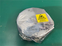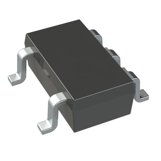
onsemi M74VHC1G125DFT2G

onsemi M74VHC1G125DFT2G electronic component

Image shown is a representation only

Manufacturer
Manufacturer No
M74VHC1G125DFT2G
Date Code
22+
Quantity
16,731
Availability
In Stock
Package
SC-88A
Packaging
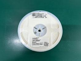
Tape and Reel
Description
Buffer/Line Driver 1-CH Non-Inverting 3-ST 5-Pin SC-88A T/R
Detailed Description
Leading the input to the transmission line this M74VHC1G125DFT2G buffer and line driver by ON Semiconductor will amplify digital and analog signals. With a 3-state output, this is power management at its best. This line driver has a minimum operating temperature of -55 °C and a maximum of 125 °C. This product will be shipped in tape and reel packaging for quick mounting and safe delivery. This non-inverting device has a typical operating supply voltage of 2.5|3.3|5 V. Its minimum operating supply voltage of 2 V, while its maximum is 5.5 V. It has 1 channels per chip.
Datasheet
ISO 13485 certification
ISO 14001 certification
Five-Star Service certification
UKAS management certification
IAF recognition arrangement certification
HTS
M74VHC1G125DFT2G
PPAP
No
EU RoHS
Compliant
Bus Hold
No
Mounting
Surface Mount
Polarity
Non-Inverting
ECCN (US)
EAR99
Packaging
Tape and Reel
Pin Count
5
Automotive
No
Lead Shape
Gull-wing
Output Type
3-State
PCB changed
5
Availability
No Stock Available
Logic Family
VHC
Package Width
1.25
Logic Function
Buffer/Line Driver
Package Height
1(Max)
Package Length
2
Supplier Package
SC-88A
Input Signal Type
Single-Ended
Tolerant I/Os (V)
5.5
Standard Package Name
SOT
Number of Inputs per Chip
1
Number of Outputs per Chip
1
Number of Channels per Chip
1
Number of Elements per Chip
1
Maximum Power Dissipation (mW)
332
Maximum Quiescent Current (uA)
1
Number of Output Enables per Chip
1 Low
Maximum Operating Temperature (°C)
125
Minimum Operating Temperature (°C)
-55
Absolute Propagation Delay Time (ns)
18
Maximum Operating Supply Voltage (V)
5.5
Minimum Operating Supply Voltage (V)
2
Typical Operating Supply Voltage (V)
2.5|3.3|5
Maximum Low Level Output Current (mA)
8
Propagation Delay Test Condition (pF)
50
Maximum High Level Output Current (mA)
-8
Maximum Propagation Delay Time @ Maximum CL (ns)
11.5@3V to 3.6V|7.5@4.5V to 5.5V
AttributeValue
HTSM74VHC1G125DFT2G
PPAPNo
EU RoHSCompliant
Bus HoldNo
MountingSurface Mount
PolarityNon-Inverting
ECCN (US)EAR99
PackagingTape and Reel
Pin Count5
AutomotiveNo
Lead ShapeGull-wing
Output Type3-State
PCB changed5
AvailabilityNo Stock Available
Logic FamilyVHC
Package Width1.25
Logic FunctionBuffer/Line Driver
Package Height1(Max)
Package Length2
Supplier PackageSC-88A
Input Signal TypeSingle-Ended
Tolerant I/Os (V)5.5
Standard Package NameSOT
Number of Inputs per Chip1
Number of Outputs per Chip1
Number of Channels per Chip1
Number of Elements per Chip1
Maximum Power Dissipation (mW)332
Maximum Quiescent Current (uA)1
Number of Output Enables per Chip1 Low
Maximum Operating Temperature (°C)125
Minimum Operating Temperature (°C)-55
Absolute Propagation Delay Time (ns)18
Maximum Operating Supply Voltage (V)5.5
Minimum Operating Supply Voltage (V)2
Typical Operating Supply Voltage (V)2.5|3.3|5
Maximum Low Level Output Current (mA)8
Propagation Delay Test Condition (pF)50
Maximum High Level Output Current (mA)-8
Maximum Propagation Delay Time @ Maximum CL (ns)11.5@3V to 3.6V|7.5@4.5V to 5.5V

Purchase & Inquiry

Placing an Order

You may place an order on DAXIN without creating an account.

Available Payment Methods

For your convenience, we accept several payment methods in USD, including PayPal, credit card, and wire transfer.

RFQ (Request for Quote)

We recommend submitting an RFQ to receive the latest pricing and inventory information for the parts you need.

Our sales team will respond to your request by email within 24 hours.

Important Notes

1. You will receive an order information email in your inbox. Please check your spam folder if you do not find the email.

2. Since inventory and pricing may change from time to time, our sales manager will reconfirm your order and notify you if any updates are needed.

Payment Method

Transaction fee is charged according to bank/payment system rules.

Shipping Method

Shipped from
Hongkong/Shenzhen warehouse
Estimated Ship Date
Oct 29, 2026 - Oct 30, 2026
Shipping Fee
Calculated based on your destination

Packages

Product before packing

Step1: Product

Product in anti-static bag

Step2: Anti StaticBag

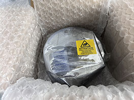
Product in individual packaging

Step3: Individual Packaging

Individual packaging box

Step4: Packaging Boxes

Packaging box with shipping label

Step5: Bar-Code Shipping Tags

Shipping by cargo vessel

Step6: Shipping